
Source Code
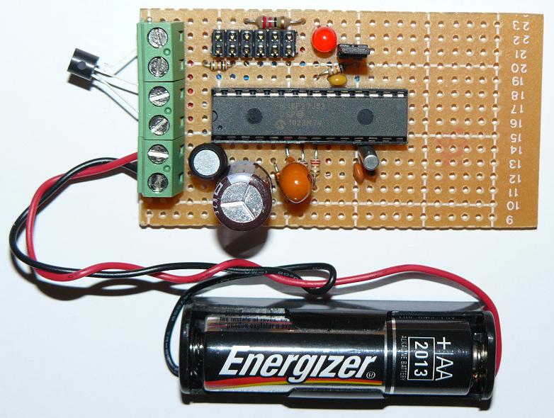
One of the design goals is to use the fewest parts need to accomplish the other goals. The reference design uses an EEPROM to store the logged data. The 24AA1025 is a rather expensive part for 128 k bytes of storage. Using a microcontroller with a large internal writeable non-volatile memory may allow this part to be eliminated. That would reduce parts cost and build time. The Microchip parametric parts selector was used to display 8 bit PIC microcontrollers in a 28 pin or smaller package. The displayed list of parts was then sorted by memory size. The highest capacity flash memory shown was 128 k bytes. That is the same capacity as the EEPROM, but some space will be taken by the firmware. The PIC18F27J53 look like a good choice. It is available in a DIP package so the logger can be easily built on solderless breadboard. It also features a real time clock (RTC) that will allow time stamps and a precise sample rate. The analog to digital converter (ADC) is 12 bits – an improvement over the 10 bits of the reference design. It also has USB that could be used to eliminate the need for the FTDI USB to serial cable. The price is 3.23 USD/qty100. The reference design used a PIC at 2.05 USB/qty100 and the 24AA1025 at 2.85/qty100 for a total of 4.90 USD. Cost savings are 1.67 USD. If this where a commercial product, there would be additional cost savings by using a smaller PCB, reduces assembly time and potentially greater reliability (fewer parts to fail.) One possible problem with using the microcontroller’s flash memory for data storage is the write cycle limit. Flash memory can be read constantly, but degrades when it is written. The number of write cycles for the PIC18F..J series parts is 10,000. EEPROMs usually allow 1,000,000 or more write cycles. If one sample is logged every second, it will take about 28 hours to fill 100 k bytes. 10,000 cycles would take more than 30 years, so this is not a problem.
The MCP9700 used in the reference design is a low cost temperature sensor will adequate accuracy. No reason to use a different part.
The reference design writes each reading to the EEPROM at the time it is read. The EEPROM allows this, but it has to read and write an entire 128 byte page just to update 1 byte. Power consumption could be reduced by buffering 128 bytes to RAM and writing whole pages to the EEPROM.
Flash memory is not as “smart” as EEPROM. It requires that memory written must first be explicitly erased. The flash memory is erased in chunks of 1 k bytes. Writing to flash is done in chunks of 64 bytes. It is not possible to write just one byte. To keep the code simple both erasing and writing will be done in chunks of 1 k bytes. 1000 readings will be accumulated in RAM. After the 1000th reading, they will all be written to flash along with up to 24 bytes of metadata. The metadata includes the real time stamp of the first reading and the absolute value of the first reading.
102 k bytes of flash are needed to store 100,000 readings. 100 k bytes will contain logged data. 1 k bytes will always be erased – this separates the head and tail of the circular buffer. The highest 1 k of flash is not used because the top 8 bytes contain the config words. It is easier to just ignore this last 1 k than to make exceptions for it. The total flash size is 128 k, so 26 k is available for the firmware.
When highest block of flash has been used, the buffer will wrap around back to the first block. The flash will always contain the latest 100,000 readings.
The next block to be used will be erased before the current block is written with the data collected in RAM. This ensures that there will always be an erased block between the head and tail of the circular buffer. If the erase fails, then the previously erased block will remain.
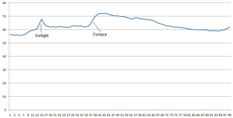
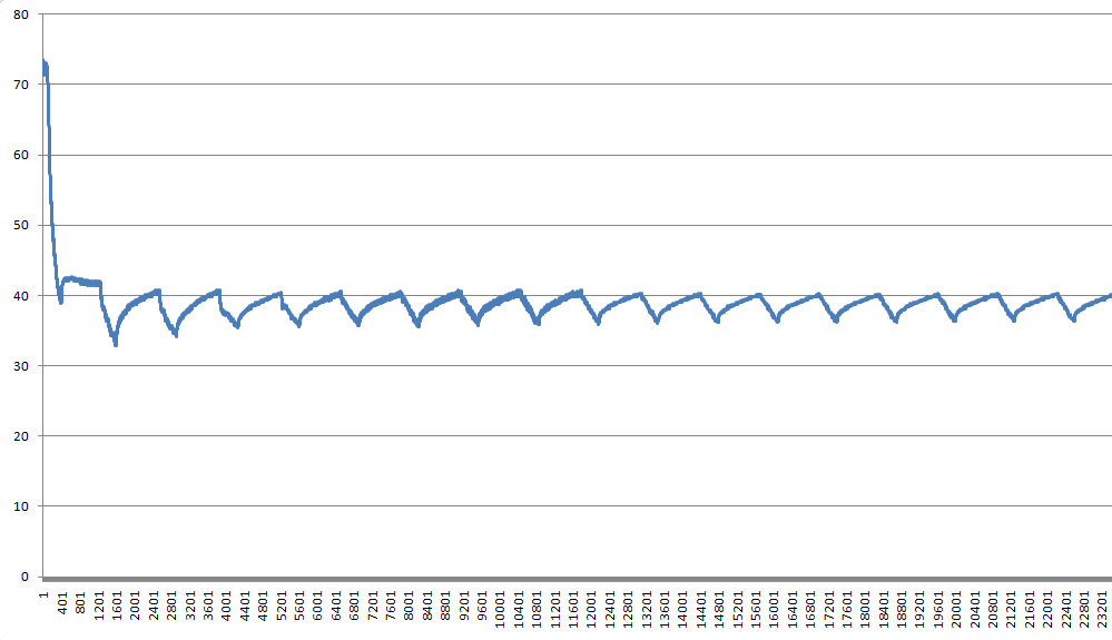
The plot below is the first dataset from the logger. Excel can not handle 100,000 rows, so only the first reading of each block of 1000 is plotted.
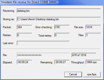
The Ymodem protocol is used to reliably transfer the logged data in binary form. This protocol is quite old and still well supported. It uses a 16 bit CRC to detect transmission errors and can handle text or binary data. Downloading the logged data is simply a matter of using terminal software to initiate a Ymodem download. A 101 k byte file named ‘datalog.bin’ will be downloaded in about 1 minute. The entire 101 k is transferred even if only part of it contains logged data. Logging does not stop during download.
The reference design converts the ADC reading to degrees C and stores that in the EEPROM. This results in a loss of resolution. A temperature of 23.4 will be stored as 23 – an unnecessary error of 0.4. If a steady slow change in temperature where plotted, it would be jagged line rather than a smooth line. Storing the actual ADC reading will preserve the full resolution of the measurement. It can be converted to whatever unit of measure is desired with whatever resolution is needed. Using the logger for something other than temperature would not require any firmware changes. Storing all 10 or 12 bits from the ADC would require more space than storing the scaled value as an integer. If the ADC reading changes by a small amount from one reading to the next, then the change in value can be stored rather than the absolute value. Eight bits will allow changes of -128 to +127 between each reading. The code is written to propagate any overflow error to the next reading. For example a change of +200 would be encoded as +127 and the error of +73 would be added to the next sample. This may result in an occasional incorrect reading, but the sequence will correct itself. It is effectively a low pass filter.
When the MCP9700 temperature sensor is used with the 12 bit ADC, the resolution of measurement is 0.06 degree C. That does not mean it is accurate to 0.06 C – it isn’t. Calibration can provide accuracy of about 1 C from 0 C to 100 C. The high resolution allows for detection of small relative changes in temperature and makes plots of the data smoother (no big steps).
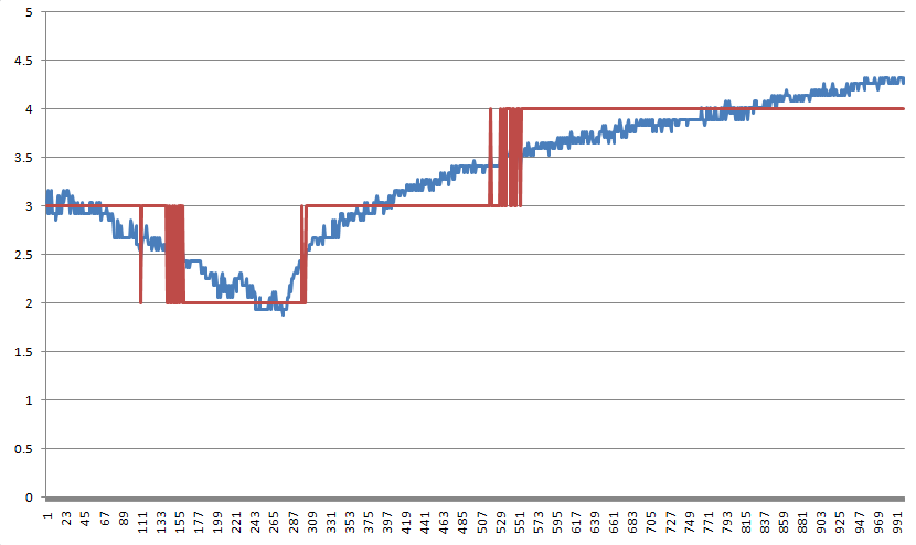
The plot below shows the same raw data converted to scaled data with 0.01 C resolution (blue) and 1 C resolution (red). The overall accuracy is the same, but the higher resolution shows the trend more clearly.
The RTC is used to provide a time stamp for the first reading of each 1000 reading block. The alarm feature of the RTC is used to set the sampling interval. A recurring alarm at a one second interval will wake the PIC from sleep. The alarm interrupt is used to ensure that logging occurs even when other code is running. The time stamp and sampling interval are from the same time source so there is no need to save a real time stamp for each reading. Adding 1 second for each reading in a block of 1000 to the initial time stamp for the block will give the correct time stamp for that reading.
Common cells like AA and AAA can easily be installed backwards in most battery holders. The orientation designations can be unclear especially for “drop in” style holders. The more cells there are in a pack, the more likely that one or more will be incorrectly installed. Using one cell allows only two possibilities – one will work and the other won’t. If the device doesn’t work, just flip the one cell – easy fix.
When current is drawn from a multi-cell battery, the individual cells discharge at slightly different rates. Over time this very small difference becomes more pronounced. If you measure the voltage of a set of 4 AA cells that are “dead”, you will likely find one of them has a much lower voltage than the other three. That relatively weak cell has limited the life of the entire pack of 4 cells. This isn’t much of a problem with primary (non-rechargeable) cells, but it is with secondary (rechargeable) cells. The weakest cell not only has different discharge characteristics, but also different charge characteristics. The number of charge/discharge cycles may be greatly limited by the weakest cell. The depth of discharge is also limited by the weakest cell. The weak cell makes the charge remaining in the other cells inaccessible. The solution is to use a charge balancer circuit to ensure that all the cells are charged equally and fully. This is a standard and very necessary part of any modern high capacity Li-Ion battery pack. For high power applications like notebook computers a multi-cell battery is the only practical solution.
For lower power applications a single cell can be used and the need for balancing circuitry eliminated. A single cell can be deeply discharged (if the chemistry allows) because there will not be a weak cell to block current flow. Using a single primary alkaline or secondary NiCd cell will allow deep discharge of the cell and maximum energy extraction from the cell.
Using solar power to supplement the battery power will result in constant charge/discharge cycles. Using a single cell battery will prevent the possibility of cell imbalance.
The power supply is the most unique feature of this design. It is an ordinary boost converter design, but does not use any external logic or power switching circuitry. It is software driven and uses 3 I/O pins as a low side switch. It is not possible for the power supply to run constantly so power is stored in a 1000 uF capacitor. The power supply will charge the capacitor whenever the RTC wakes it to take a reading.
Microcontroller driven switching power supplies are not unique. They usually use the PWM peripheral to drive an external power switch (usually a MOSFET). The output voltage can be read by the ADC and used the adjust the PWM duty cycle to achieve regulation. Using a microcontroller can reduce parts count and product cost.
I didn’t know if the usual MOSFET could be eliminated. The I/O ports of the PIC are not fully characterized. The spec sheet specified the voltage drop at a specific current, but does not have any V/I curves or other specs. The point of transition from the ohmic region to the saturation region is unknown. It is very desirable to stay in the ohmic region (low Rds) because losses are significant in the saturation region. The digital only pins seem to be the best choice because they are clearly stronger than the analog/digital pins. The analog/digital pins can only suppy 8 mA at 400 mV, while the digital only pine can supply 25 mA at 400 mV.
A circuit was built on a solderless breadboard to test the power supply design. It worked as expected and was able to supply 3.5 volts from a 1.5 volt AA battery. The High Low Voltage Detect (HLVD) module of the PIC is used to detect when the supply voltage reaches 3.5 volts. The supply will then shut down and the PIC will run with power stored in the 1000 uF capacitor. Code was written to test the power supply by using the HLVD to detect when the voltage falls to 2.5 volts and then boost it back up to 3.5 volts. This test code worked as expected. The voltage would rise to 3.5 volts and then fall to 2.5 volts several times a second.
The test code was modified to sleep while waiting for the voltage to fall. The PIC should be able to sleep for quite some time on the charge stored in a 1000 uF capacitor. This did not work as expected. The cycle was still rapid despite the PIC sleeping after the capacitor was charged. The test circuit was connected to a bench supply and oscilloscope to investigate the problem. The bench supply was set to 2.5 volts to “jump start” the system. The circuit was able to sleep for a long time when supplied with 2.5 volts. The voltage was slowly lowered to 2.0 volts and everything kept working well. As the voltage was decreased below 2.0 volts the problem reappeared – the sleep time was very short. The problem was leakage in the PIC’s I/O port. When the voltage on a digital only I/O pin is between a distinct logic high and logic low there will be excessive current flow. The fix was to use analog/digital pins rather than digital only pins. The leakage problem was solved and the PIC can sleep for about 5 minutes. The calculated current draw during sleep is about 3.5 uA.
The bench supply was used to determine the lowest voltage that could support fully charging the capacitor to 3.5 volts. With the simple fixed pulse width code the lowest voltage was 1.0 volts – higher than I wanted. The code was modified to charge the inductor until the output port saturated. The comparator module is used to detect saturation. The discharge time will be shorter for longer charge times because a slow charge occurs at low voltage and there will be less power stored in the inductor so less time is needed for discharge. The circuit would operate down to 700 mV after these changes.
It was very clear that the output port could not sink enough current to allow operation below 700 mV. Using an external MOSFET would probably allow operation down to 600 mV. Not enough gain to justify an additional component.
This unique power supply design requires a “jump start” to get it going. The PIC needs power to make more power. Power is taken from the FTDI USB to serial cable to get the system up and running. The cable supplies 5 volts from USB, but the PIC needs 2.5 to 3.5. A voltage regulator is the obvious solution, but would require several more parts. An ordinary red LED is used to drop the 5 volt USB power down to about 3 volts. A 22 ohm resistor limits inrush current. The LED also indicates when the PIC is using power from USB – it goes out when the PIC sleeps. There is no need for battery power when USB power is available, so the external HLVD input is used to quickly detect when USB power is available and the battery will not be used.
The plot below is from the refrigerator. It was done after debugging the power supply. The logger was powered by a “dead” AA battery that was no longer able to power a cordless mouse.
Power can easily be supplemented by solar cells. A single AA or AAA NiMH battery can be charged with small 4 cell solar panel. There is no need for any charge regulation as long as the maximum possible charge is less than 0.1 C (1/10 cell capacity). There will be no cell balance problems because there is only one cell.
Another way to supplement power with solar cells is with an 8 cell solar panel connected to C1. This will keep C1 charged to almost 4 volts when sufficient light is available. The boost converter will not run if C1 is already fully charged. This is more efficient than charging the battery from solar, but requires more cells in the solar panel.
Using internal flash memory and RTC reduces power consumption relative to using external parts. When external parts are used, the microcontroller has to spend time waiting for the relatively slow IIC or SPI communication with the peripheral. Access to internal resources is very fast, so no power is wasted waiting for communication to complete.
Optimizing code for speed will also optimize for power consumption. The less time spent doing something, the less power will be used. Using C to write embedded firmware is quite popular. It allows for rapid development and some portability. Using a high level language allows the programmer to focus on the concept rather than the implementation details. The C compiler will try to generate optimal assembly code, but there is opportunity to improve performance by writing code that allow maximum optimization. Understanding the hardware’s capabilities and instruction set can provide insight into writing optimal C code.
Here is some code that is written in a very straightforward and reasonable way.
WriteFlashPage(unsigned char rom *page, unsigned char *data)
{
  int i, j;
  for(i = 0; i < 16; i++) {
    for(j = 0; j < 64; j++) {
      page[i * 64 + j] = data[i * 64 + j];
    }
    WriteBlock();
  }
}
There are a few easy optimizations that can greatly improve the performance. Using an int for loop iteration is common and reasonable. For a microcontroller like the PIC18 series, it is inefficient. The ALU is 8 bits, so using a 16 bit int will generate more code and run slower. Using an 8 bit char will make the code smaller and faster. Using unsigned values rather than signed may also offer performance improvements in some cases. Using a for() loop is also common and reasonable, but may not be optimal. A do/while() loop may be faster if loop termination is decided by a simple test.
The array index requires a multiply and add. Simply incrementing a pointer would be much faster. The PIC18 has one program memory pointer and three data memory pointers. They all support postincrement operations.
This revised code is smaller and faster. 16 bit integers have be replace by 8 bits unsigned chars. The loop termination is a test for zero after predecrement, rather than a test for a specific non-zero value. This can be done with the decfsz instruction. The array index calculation is gone, replaced by postincrement pointer operations.
WriteFlashPage(unsigned char rom *page, unsigned char *data)
{
  unsigned char i, j;
  i =  16;
  do {
    j = 64;
    do {
      *page++ = *data++;
    } while(--j);
    WriteBlock();
  } while(--i);
}